High-density power modules simplify and downsize EV power system design
Vicor power modules infuse innovation into EV applications. Learn how three new automotive-grade products will revolutionize the future of power designs
For a graphic illustration of why power sequencing is essential, consider what could happen in a large industrial system if its motors and actuators became energized before its control electronics. Clearly, the potential for such unpredictable and dangerous scenarios must be eliminated with carefully-designed power start-up sequences. And shutdown sequences are equally as important.
Incorrect power sequencing can cause problems at the semiconductor as well as at the system level: these conditions could lead to unexpected reverse bias across a CMOS device. This can damage or destroy the device, or latch it into an ON state that can only be released by power cycling. Although blocking diodes can prevent latch-up, they can limit the usable analogue input voltage range, so supply voltage start-up sequencing is the preferred solution. Additionally, multi-voltage devices such as DSPs and microprocessors usually require their I/O voltage to be present before applying the core voltage. Intel processor chip documentation typically specifies start-up and shut-down sequences that must be followed. Similarly, CPU chips must be powered up before systems graphics ICs to prevent uncontrolled outputs to the graphics display.
There are two typical approaches to power sequencing; one based on power and the other on logic.
The Power solution uses the voltage rise in one power rail to send a suitably delayed trigger signal to an N-channel MOSFET, which controls the supply to the second power rail. The Logic approach is based on using Enable or other logic pins on power train devices rather than controlling the power to them. Using the logic integrated in power components provides a lower-cost, more compact and simpler solution, but in more demanding applications, MOSFETs permit more accurate control of turn-on time.
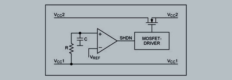
Fig 1 below shows a basic MOSFET sequencing circuit using an N-channel MOSFET and a comparator. VREF sets the threshold for switching VCC2, with VCC2 turning on after VCC1 with a delay set by the RC network. The MOSFET driver includes a charge pump to ensure that VGS exceeds VCC2 by several volts; this fully enhances the MOSFET switch. This circuit also ensures that VCC2 shuts down when VCC1 does, however the RC network means that VCC2’s shutdown will lag VCC1’s. Another issue can arise if VCC1 is not available for use as a reference voltage.
Figure 1 – Power sequencing using an RC network, comparator and MOSFET driver
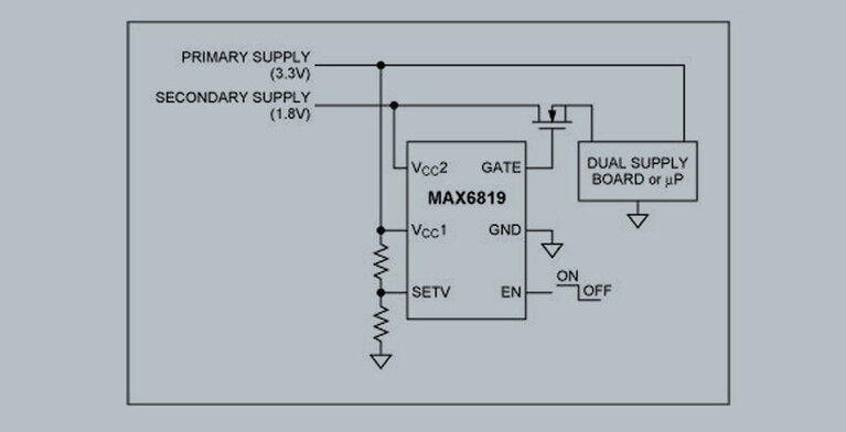
More highly integrated and easier solutions are available, such as the example shown below in Figure 2.
Figure 2 – Power sequencing with the MAX6819
The sequencer ensures that the MOSFET always has the minimum required VGS enhancement, which minimizes loss in the MOSFET and ensures a low drain-to-source impedance (RDS(ON)). The MAX6819 imposes a factory-set delay time of 200ms, which occurs after the primary voltage rises above the set threshold and before enabling the charge pump to drive the external MOSFET switch.
Vicor voltage regulator, VI Chip and Brick products can be sequenced by the MOSFET circuits above. Alternatively, they can often be managed through their control pins and internal logic as mentioned earlier. In one simple arrangement, a ‘soft start’ output from one device can be connected to the logic enable/disable pin of another, effectively controlling its power sequencing. Additionally, many Vicor devices have a voltage control pin, or trigger. If a ramp voltage is applied to this pin, the device’s output will ramp to track the voltage control input, but with a fixed time delay.
High-density power modules simplify and downsize EV power system design
Vicor power modules infuse innovation into EV applications. Learn how three new automotive-grade products will revolutionize the future of power designs
Active suspension comes of age bolstered by high-density power modules
Active suspension has evolved from 1990s beta model to today’s 48V-driven system. See the impact power modules have made on power system design
Advanced power module packaging optimizes available power, reliability and safety in autonomous electric shuttles
Vicor high-efficiency power modules ensure minimal heat dissipation, reducing the need for complex cooling solutions and maximizing power
MHz switching frequency-based devices enable miniaturization of the DC-DC converter and EMI filters
Imagine using DC-DC converters solutions to harness the benefits of high-frequency switching without incurring conventional shortcomings


