


High-bandwidth power modules quell the disruption of high-voltage line ripple rejection
Vicor DC-DC converters combine high bandwidths with soft switching topologies to reduce EV ripple rejection more effectively than conventional solutions
Capacitance at the input of the DC-DC converter plays a vital role in keeping the converter stable and playing a role in input EMI filtering. Large amounts of capacitance at the output of the DC-DC converter can provide significant challenges in the power system. Many loads downstream of the DC-DC converter need capacitance for proper operation. These loads can be pulsed power amplifiers or other converters that need capacitance at their inputs. If the capacitance at the load exceeds the value that the DC power system is designed to handle, the power system can exceed its maximum current rating at startup and during normal operation. The capacitance can also cause power system stability issues and lead to improper system operation and premature power system failure.
A few simple techniques can be implemented within the power system to maintain an efficient and reliable design when powering highly capacitive loads. Reducing the voltage rise time across the load capacitor at start up will keep the power system within its current rating, controlling the charge current into the capacitor during operation will keep the power system within its power rating and adjusting the control loop of the system will keep the power system stable and within system voltage ratings.
At start up, the typical DC-DC converter has a standard rise time set by the rise of an internal error amplifier reference. A discharged capacitor placed at the output of the converter will appear as a low impedance load. With this low output impedance, a few switching cycles of the converter can cause a change in voltage across the capacitor high enough to force the converter to exceed its output current rating. The capacitor can be pre-charged through a higher impedance path at the output of the converter. This high impedance element will limit the charge current into the capacitor until the capacitor is charged to a pre-defined voltage level. Once the pre-defined voltage level is reached, the high impedance path can be removed or shorted by a low impedance device such as an FET.
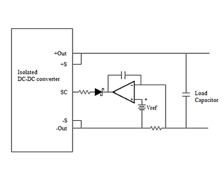
The converter can deliver its full rated current through this lower impedance path. When the FET shorts the impedance path, the full voltage of the converter is allowed to charge the capacitor. The turn on time of the FET and the voltage differential between the capacitor and the converter voltage will determine the charge current needed to bring the capacitor to full voltage and thus it is important to set the pre-defined voltage level to a point where the FET turn on does not cause the converter to exceed its current rating. The block diagram in Figure 1 can be used to charge a capacitor to a preset voltage minimum. U2 controls the FET that shorts the impedance Z and the U1 circuit works in conjunction with U2 to set the turn on voltage and the load enable.
Figure 1: Capacitor pre-charge block diagram
Figure 1: Capacitor pre-charge block diagram
At start up the converter will see the capacitor as the load as well as the system loads after the capacitor. If the system load is demanding current from the capacitor during the high impedance pre-charge, the capacitor may not achieve the pre-set charge voltage. Many downstream loads to the DC-DC converter have an under voltage lockout, under which they will demand little current. If the load does not have an under voltage lockout above the pre set charge voltage then an external Enable should be used. If the load is resistive in nature, a series switch can be used to enable voltage to load after the capacitor is charged. Figure 2 shows the voltage and current of a system charging a 10mF capacitor.
Figure 2: 12VDC converter charging a 10KµF capacitor
Figure 2: 12VDC converter charging a 10KµF capacitor
Once the capacitor is charged the load can begin to draw current from the capacitor and DC-DC converter. There are loads that demand current rapidly and the current will be delivered by the capacitor if the demand is outside the converters bandwidth. Once the current is delivered by the capacitor the voltage across capacitor drops:

Where Vdrop is the voltage drop across the capacitor, I is the current demand, C is the capacitor value and dt is the duration of the current draw. The converter will recharge the capacitor to its original value and in doing so, the converter can exceed its current rating. The voltage differential between the converter and the depleted capacitor divided by the resistance between the two voltages will determine the desired recharge current. The resistance between the two voltages is typically very low to reduce system losses and thus the desired recharge current can be higher than the converter maximum. Because the voltage of the capacitor is near the set point voltage of the converter, exceeding the converters maximum current can also exceed the converter’s power maximum.
To keep the converter from exceeding its current and power ratings during normal operation, the current control block diagram in Figure 3 can be used to control the re-charge current after a high di/dt event. The circuit monitors the current across a shunt resistor and limits recharge current by actively trimming down the voltage of the converter. The limited voltage differential between the converter and the capacitor will limit the capacitor recharge current to keep the converter within it current and power limits. As the capacitor voltage rises, the converter voltage rises until it reaches its set point.
The current limiting method shown in Figure 3 can be used in conjunction with the pre- charge method in Figure 1 allowing for a faster start up. The pre-charge can charge the capacitor to the minimum trim voltage of the converter and then the converter can fully charge the capacitor with its full current rating. Controlling the rate of rise of the output voltage will control the current charging the capacitor. However, most DC-DC converters have a narrow control or trim range from their nominal set voltage. A typical trim range is +/-10%. There are some manufacturers that have a wider trim range where the converter can be trimmed down to -90% of the nominal set voltage. The lower the voltage trim range, the lower the need for an enable circuit as downstream loads typically have a under voltage lockout close to their operating voltage minimum.Figure 3: External current limiting block diagram
Figure 3: External current limiting block diagram
Once the converter is kept within it limits at start up and during operation, we must now ensure system stability. A large capacitor at the output of the DC-DC converter can degrade the phase margin of the system and cause oscillations. To ensure that the converter is stable there must be a minimum amount of impedance in series with the capacitor. The lead or trace impedance, the FET ESR and the ESR of the capacitor contribute to this impedance. The best way to find the minimum value for this impedance is to use a network analyzer and run a system analysis to determine the phase and gain margin. If a network analyzer isn’t available, a load step can be applied to the system and the converter voltage and current wave forms can be analyzed to ensure that there isn’t excessive ringing which is a sign of poor stability.
Once the voltage loop is stable the current control loop in Figure 3 can be examined for its contribution to the system stability. This current control loop is within the control loop of the DC-DC converter and should have a bandwidth well below the systems loop crossover frequency so the two loops don’t interact. In converter systems where the power train’s compensation network is enclosed within the converter, the converter manufacturer can provide enough information to set a suitable cross over frequency for the current control loop. There are some converter manufactures that give the designer the ability to adjust the power train control loop to optimize the performance for a particular application. Figure 4 shows a converter with an external control loop. The control loop can be optimized to provide peak system performance. This external control loop can be vital in applications were the power system’s response time in critical for proper system operation. This is the case in a periodic pulsed load application where the converter has to recharge the capacitor before the next power pulse. The system stability should be verified with either a network analyzer or a step load test. Systems that are unstable can have voltage excursions that exceed the power system component ratings and can eventually lead to power system failure.Figure 4: Converter with external control loop
Figure 4: Converter with external control loop
High-bandwidth power modules quell the disruption of high-voltage line ripple rejection
Vicor DC-DC converters combine high bandwidths with soft switching topologies to reduce EV ripple rejection more effectively than conventional solutions
High-performance power modules drive mission critical ‘seeing’ sensors
Kodiak Robotics’ self-driving technology to revitalize trucking industry
The future of standardized defense platforms using MOSA, SOSA and VPX open architectures
Using open standards to increase interoperability, scalability, reliability, reduce system costs, and minimize the number of custom electronics designs
Delivering higher power density and low noise for New Space applications
Patented power design techniques and architectures needed to deliver optimal power and low noise for space communications applications


