


HIRO pushes Europe to the edge with high-performance microdata centers
From supporting brain surgery to driving smart factories while saving power—HIRO is driving Europe to the edge with innovative computing concepts
While genAI holds the promise of increasing human productivity, it comes with staggering energy and greenhouse gas costs. Today Vicor power modules combined with a vertical power delivery architecture offer the most efficient approach to powering genAI and unleashing industry-leading current density.
By Maury Wood, VP Strategic Marketing, Vicor
Training generative AI (genAI) neural network models typically take months, with thousands of multi-billion-transistor GPU based processors, high-bandwidth SDRAMs, and terabit per second optical network switches operating simultaneously and continuously. While genAI holds the promise of increasing human productivity, it comes with staggering energy and greenhouse gas costs.
The New York Times reported that by 2027, AI servers could use 85 to 134 terawatt hours annually – roughly the yearly electrical energy consumption of Argentina.
To restrain this escalating energy consumption, power delivery networks for AI processors have undergone a multi-generational evolution. This comprehensive adaptation has involved innovations in circuit architecture, power conversion topologies, materials science, packaging, and mechanical/thermal engineering.
From 2020 to 2022, the Thermal Design Power (TDP), a measure of continuous power dissipation of the GPU-based engines used in genAI training applications, nearly doubled, from 400W to 700W. Since 2022, the semiconductor industry has seen a continued rise in TDP levels, and in March 2024 > a GPU with a 1,000W TDP was announced.
The chiplet-based processor complexes used for genAI training are composed of a GPU or ASIC die, plus six to eight High-Bandwidth Memory (HBM) dice. The GPU, which in 4nm CMOS typically operates at a core VDD of 0.65V, might have 100 billion or more transistors. The HBMs, which might comprise 144 Gbytes, and typically operate with supply voltage of 1.1V or 1.2V. One of the key power supply characteristics of the processor relates to artificial neural network algorithmic loading. There can be an enormous change in transient current consumption (dI/dt) between the GPU in an idle state and the GPU in a fully algorithmically loaded state, as high as 2,000 amps per microsecond or more. Also, the processor cannot tolerate large supply voltage undershoot or overshoot amplitudes; typically, these load step transients must be limited to 10% or less of the nominal VDD. Because of these dynamic operating conditions, the power delivery solution for training genAI processors is typically designed with a peak current delivery capacity that is > twice the continuous current delivery capacity, with the peak events generally lasting tens of milliseconds (Figure 1).
Figure 1: GenAI training GPU-based processor chiplet complex with high bandwidth memories (HBMs) mounted on an accelerator module (AM).
The foremost power delivery architecture that has evolved for CPUs, FPGAs, network switch processors, and now AI training and inferencing chips is the Point of-Load (PoL) approach. Factorized PoL current multiplication approach achieves much higher power and current density than traditional multi-phase voltage averaging. This power architecture leverages the concept of an idealized transformer “turns ratio”, in which voltage division yields current multiplication. The scalable nature of current multiplication enables the development of a comprehensive family of PoL converters, at different output voltage levels and output current levels. This is critically important for customers, as the requirements of advanced AI training processors are changing rapidly.
Summarizing the trending challenges for genAI power system design:
Solving this high-current and high-density point-of-load (PoL) problem requires a different approach. The state-of-the art Factorized Power Architecture disaggregates or factorizes the regulation and voltage transformation/current multiplication functions to allow these power delivery stages to be optimally placed and achieve the highest possible efficiency and power/current density.
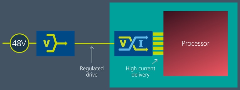
A regulator has optimum efficiency when VIN = VOUT and loses efficiency as the regulator's input to output ratio increases. With a typical input voltage varying between 36 and 60V, the optimum output bus voltage would be 48V instead of the legacy 12V bus that is typical of Intermediate Bus Architecture (IBA). A 48V output bus requires four times lower current than the 12V bus (P = VI) and PDN losses are the square of 2 the current (P = I2R), which reduces losses by 16 times. So, placing the regulator first and regulating to a 48V output will achieve the highest efficiency. The regulator must accept an input that can sometimes swing lower than 48V, necessitating a buck-boost regulating stage to satisfy this aspect of the design. Once the input voltage is regulated, the next step is to convert the 48 to 1V.
In the case of a 1V load requirement, the best transformation ratio would be 48:1. In that case, the regulator bucks or boosts the input to a 48V output and the transformer steps down the voltage from 48V to 1V. Given that a step-down volt age transformer increases current by the same ratio, an equivalent name for the transformer component is a current multiplier. In this case, a 1 amp input current would be multiplied to 48 amp out. To minimize PDN losses of the high current output, the current multiplier needs to be small so it can be positioned as close to the load as possible.
PRM™ Regulators and VTM™/MCM™ Modular Current Multipliers combine to form the Vicor Factorized Power Architecture. These two devices work in partnership with one another, each fulfilling its specialized role efficiently to enable the complete DC-DC conversion function.
The PRM supplies a regulated output voltage, or “factorized bus” from an unregulated input source. This bus feeds a VTM which transforms the factorized bus voltage to the level needed by the load.
Unlike IBA, FPA does not step down from an intermediate bus voltage to the PoL through series inductors. Instead of averaging down the intermediate bus voltage, FPA uses high-voltage regulation and current multiplier modules with a current gain of 1:48 or higher to provide higher efficiency, smaller size, faster response and scalability to 1000 amps and beyond (Figure 2).
Figure 2: The Factorized Power Architecture™ can deliver a high current of greater than 1000 amps and enable a 20X reduction in power delivery network resistance.
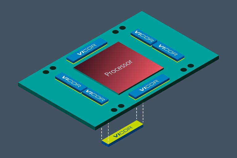
In the first few generations of high-current genAI processor power architectures, the PoL converters were physically placed lateral (adjacent) to the processor complex. The Power Delivery Network (PDN) of a laterally-placed PoL solution has a lumped impedance that is fairly high, perhaps 200μΩ or higher, due to the resistivity of copper and the length of the traces within the PCB. As continuous current requirements for genAI training processor increase to 1,000 amps, this is 200 watts of power dissipated in the PCB itself. When multiplied by the thousands of accelerator modules (AMs) used in AI supercomputers for large language model training, this 200 watts becomes very substantial, particularly consider that the AMs are almost never powered down; they typically run 24/7 for ten years or more.
In recognition of this wasted energy, AI computer designers have begun to evaluate the placement the PoL converters directly below the processor complex, in a Vertical Power Delivery (VPD) structure. In a VPD PDN, the lumped impedance might be 10μΩ or less,
which dissipates 10 watts at 1,000 amps continuous for the core volt age domain. This is a 200 – 10 = 190W (WPCB) reduction in PCB power dissipation by moving from lateral PoL converter placement to vertical PoL converter placement (Figure 3).
Figure 3: GenAI acceleration module with both lateral (top side) and vertical (back side) power delivery for up to 20X reduction in PDN losses.
Another merit of VPD is a reduction of GPU die surface voltage gradients, which also leads to power savings. As mentioned, a typical 4nm CMOS GPU nominal operating voltage is 0.65VDD. Using lateral power delivery, with power applied to the four side edges of the processor complex, a voltage of 0.70V may be required to ensure 0.65V nominal at the GPU die center, due to the integrated circuit power distribution impedance (which typically uses aluminum conductors; aluminum has a resistivity higher than copper). With vertical power delivery, 0.65V can be assured across the die surface. This difference of 0.70 – 0.65 = 50mV, multiplied by 1,000 amps, yields an additional 50 Watt (WVDD) of power savings. In this example, the total power dissipation saving is 190 WPCB + 50 WVDD = 240 watts (Figure 4).
Figure 4: Uniform voltage across processor die surface with VPD, maximizing compute performance while minimizing power losses.
Using public domain demand forecasts of AMs in the coming years (more than 2.5M units in 2024), and using reasonable estimates of the economic cost of electrical power ($75 USD per Megawatt hour), this 240W savings per AM leads, by 2026, to Terawatt-hours of power savings at the global level, equivalent to billions of dollars of electrical operating costs, and millions of tons of carbon dioxide emissions reductions (depending on the renewable energy mix) annually and in perpetuity.
Vicor is working at the leading edge of this evolution in genAI power delivery. Factorized Point of Load converter solutions help to improve genAI processor power efficiency, to better align genAI power consumption with societal-level environmental and conservation goals. Vicor is continuously innovating > new power architectures and developing advanced new products to help mitigate the escalating power consumption associated with genAI model training. With an advanced factorized current multiplier approach to PoL DC-DC conversion, the benefits of genAI can be delivered while limiting associated power consumption at the global level.
This article was originally published by Power systems Design.
Maury Wood is Vice President of Strategic Marketing at Vicor Corporation. Prior to joining Vicor, Maury held senior roles at optical fiber test and semiconductor companies, including EXFO, AFL, Broadcom, NXP, Analog Devices, and Cypress. He holds a BSEE from the University of Michigan and did graduate studies at Northeastern University, Babson College, and MIT. He enjoys climbing, back-country skiing, mountain biking, and playing jazz bass.
Maury Wood, VP Strategic Marketing
Computing solutions: Power solutions that maximize AI, HPC and data center computing performance
Powering innovation: Redefining 48V to PoL regulation for high-power processors and AI ASICs
Article: Vertical power delivery enables cutting-edge processing
Partner podcast: Powering the high-performance compute market
Article: High-performance computing power FAQs
HIRO pushes Europe to the edge with high-performance microdata centers
From supporting brain surgery to driving smart factories while saving power—HIRO is driving Europe to the edge with innovative computing concepts
Powering the future: Innovations in GenAI power delivery
How staggering are the power requirements of large language models? What can be done to reduce power consumption? Learn what modular power can do
The importance of edge computing
Faster speeds are becoming critically important. Learn what applications are thriving and why power density is so critical to future growth
With AI innovation comes power challenges
Powering genAI is taxing software, hardware and environmental basics. Power modules help achieve higher current density, minimizing the overall impact.