


Powering the future: Innovations in GenAI power delivery
How staggering are the power requirements of large language models? What can be done to reduce power consumption? Learn what modular power can do
The massive data volumes generated by demanding AI training models is exceeding processing capacity. To enable peak compute performance without blowing one’s energy budget, a new approach to data center power distribution is needed. Learn why Vicor Vertical Power Delivery is the most efficient approach for today’s machine learning.
A Q&A with Maury Wood, VP of Strategic Marketing
Generative artificial intelligence (genAI) has been growing in popularity, but its hunger for compute cycles requires lots of power. Addressing the power requirements of large-scale genAI can be challenging. Electronic Design’s Bill Wong talked with Maury Wood, Vice President of Strategic Marketing at Vicor Corp., to get insight into the challenges and solutions.
OpenAI introduced ChatGPT in November 2022, and the resulting cultural impact (and the anticipated forward-looking impact) of genAI is monumental, eventually expected to touch every aspect of human activity. From a technology viewpoint, one thing is increasingly clear: GenAI model training will drive the highest possible levels of compute performance, storage capacity, and network bandwidth.
GenAI is motivating massive levels of new investment in the semiconductor, infrastructure hardware and system software, and network edge sectors. And this investment activity can be expected to spread into embedded AI devices for vehicles, homes, and workplaces.
GenAI training processors today use a huge number of transistors—100 billion or more—in advanced technologies such as 4-nm CMOS chiplets, which leak current during operation. Even though the supply voltage of these transistors is as low as 0.7VDD, the continuous current demand can be 1,000A or higher, putting continuous power (also known as thermal design power) at 700W. Peak current demand can run as high as 2,000A, which equates to peak power of 1,400W or more for short durations.
GenAI inferencing uses much less power. A good rule of thumb is the energy cost of inference is about the square root of the energy cost of training the same large language model (LLM) (Figure 1).

Figure 1: Progression of genAI training processor peak current requirements.
This challenge relates to the fact that electrical current demand is highly transient, depending on the algorithmic loading of the training processor. In other words, as neural-network model task loading increases or decreases, the current requirements swing quite dramatically, as much as 2,000A per microsecond.
Furthermore, to avoid transistor damage during these frequent transient events, any supply voltage overshoot or undershoot must be limited to less than 10% (or 0.07V at 0.7VDD). This is very challenging for traditional power-delivery architectures.
Until fairly recently, data centers have used 12VDC power distribution. Vicor, over the past 10 years, has advocated for the use of 48VDC power in data-center racks, because (thanks to Ohm’s Law) higher voltage yields lower power losses in conductors with non-zero electrical resistance. The adoption of 48VDC power for higher-performance computing applications received a major boost in the Open Rack specifications standardized by the Open Compute Project.
In early genAI power-distribution architectures, this nominal 48VDC supply is converted into an intermediate bus voltage at the accelerator module. This intermediate DC signal often feeds multiphase trans-inductor voltage regulators (TLVRs), an approach that has hard limits in terms of scalability and current density.
The printed-circuit-board (PCB) space available on the accelerator modules (AMs) used with genAI training processors is extremely limited, meaning that the power-delivery subsystems for these processors must have very high power density (W/mm2) and current density (A/mm2). Traditional power supplies simply can’t achieve the power and current density required to both supply the needed current and fit easily within the available PCB area.
As mentioned, the power components for genAI training processors must meet the dynamic performance demands caused by load-step transients. Again, conventional power-delivery approaches are not well-suited to those demands, particular since genAI training processors need about 3mF of decoupling capacitance as close as possible to the processor package (Figure 2).
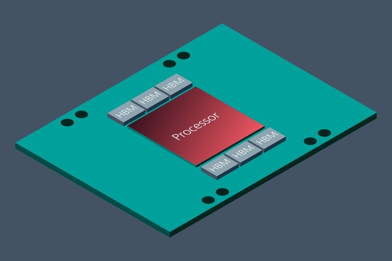
Figure 2: This conceptual genAI accelerator module, which shows the genAI processor, supports high-bandwidth memories (HBMs) using chiplet packaging.
In addition, the components in a genAI power-delivery architecture must be highly thermally adept. Whether the genAI system is liquid- or air-cooled, the power components must have high thermal conductivity and packaging that can withstand extraordinarily high levels of thermal cycling over its operating life.
More recent genAI AMs use a factorized power architecture, with the point-of-load converters utilizing current multiplication, such as those innovated by Vicor.
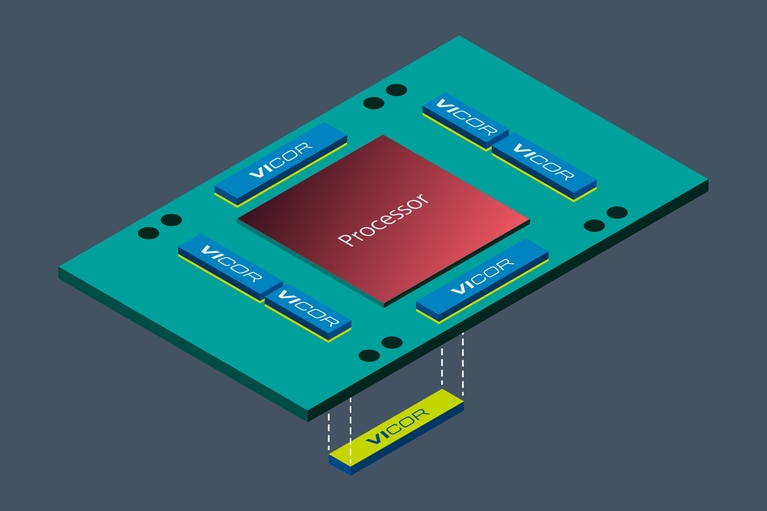
One important approach to reducing genAI power consumption, while enhancing the quality of the power delivery, relates to the physical placement of the point-of-load power components. By moving these final-stage power components from lateral placement to vertical placement directly beneath the genAI processor, the amount of power dissipated in the PCB itself is reduced. With current density of around 3A/mm2, the point-of-load current multiplier can share the very limited space beneath the genAI training processor.
This PCB thermal power reduction is possible because the lumped impedance of the vertical power-delivery (VPD) network is decreased by as much as a factor of 20 as compared to a pure lateral power component placement.
At present, the largest genAI training supercomputers deploy as many as 20,000 accelerator modules. Remarkably, according to NVIDIA, OpenAI’s GPT-3 with 175 billion parameters requires about 300 zettaFLOPS (1021 floating-point operations per second), which is 300,000 billion-billion math operations across the model’s entire training cycle. These model sizes are only going to increase, with trillion-parameter neural-network models in development today.
Vicor estimates that factorized VPD can save about 100W per accelerator module versus traditional TLVR lateral power delivery (bear in mind that AI supercomputers are energized essentially in perpetuity, meaning that they’re never powered off).
Making reasonable assumptions about the number of genAI data centers in operation globally by 2027, Vicor estimates an aggregate saving of terawatts of power, equivalent to billions of dollars of electrical energy costs and millions of tons of carbon-dioxide reductions annually, depending on the renewable-energy mix (Figure 3).
Figure 3: Laterally and vertically placed power components in the accelerator module helps minimize PDN losses.
Multiphase pulse-width-modulated (PWM) buck voltage regulation can be conceptualized as current averaging, similar to creating warm water with a dynamic mix of hot (full peak current) and cold water (no current). Vicor Factorized Power Architecture is fundamentally different and can be conceptualized as high-efficiency voltage division yielding current multiplication.
Modular current multiplier converters housed in package (ChiP™) products are PCB-layout-compatible to achieve a wide range of levels of current delivery without significant engineering rework.
This industry-leading power-delivery architecture is combined with a state-of-the-art sine amplitude converter (SAC™) circuit topology, which uses zero-voltage switching and zero-current switching methods to minimize switching noise and spurious radiated emissions and maximizes DC-DC conversion efficiency. High-frequency MOSFET switching reduces the physical size of highly integrated modules. These design elements combine with advanced components and packaging to address next-generation AI/HPC current delivery challenges.
Leading semiconductor manufacturers such as TSMC have disclosed their technology roadmaps for the next two or three process nodes (2nm, 1.6nm) utilizing new CMOS innovations such as gate-all-around nanosheet or nanowire transistors. These enhancements in device physics and the accelerating use of chiplet packaging will continue to drive ever-higher current levels for genAI processors.
On the algorithm development side, it’s virtually assured that the major LLM developers such as OpenAI, Microsoft, Google, Meta and Amazon will press forward with multi-trillion parameter neural-network models, demanding ever-higher compute, storage, and network communication bandwidth.
GenAI will, without doubt, remain the most power-intensive and thermally challenging application in the modern computing world for the foreseeable future. Vicor will continue to innovate to meet the escalating power-delivery requirements of this exciting new business opportunity.
Yes, mostly because it can be reasonably expected that businesses and individuals will demand enormous amounts of inferencing bandwidth in the medium to long term. Many, if not most, genAI applications will use pre-trained models, purpose-adapted using prompt engineering. Training cycles will be relatively infrequent (many orders of magnitude less common) compared to inferencing cycles.
Cloud service providers (CSPs) will look for the lowest-cost inferencing solutions. These require both integer- and vector-oriented instruction (floating-point multiply-accumulate operation) to be supported.
The CSPs will want to run as many inferencing tasks simultaneously as possible, driving their processor architecture selection toward high-core-count, high-bandwidth compute engines with high trillions of operations per second (TOPS) per-watt performance metrics. High-bandwidth inferencing processors have been announced, and some specify TDP levels up to 500 W. We can expect to see this trend continue and accelerate moving forward.
All of the genAI training processors announced over the past couple of years use chiplet packaging technology. The use of heterogeneous logic and memory chiplets has allowed processor developers to push past the recently diminishing returns of both Dennard scaling and Moore’s “Law,” which together enabled semiconductor manufacturing technology to progress so dramatically over the past 70 years, from 20mm to 2nm feature size.
GenAI chiplet solutions typically combine high-bandwidth-memory (HMB) devices with graphics processing units (GPUs) on a single substrate, with wide and fast bus connections. TSMC recently announced a chip-on-wafer-on-substrate (CoWoS) roadmap that leads to 120– × 120mm substrate size, which is expected to consume several thousand amps. Recent wafer-scale genAI training processors from Cerebras (CS-3) and Tesla (Dojo D1) consume about 23kW and 15kW, respectively.
For the foreseeable future, it appears genAI processors power levels will continue their stunningly rapid growth.
This article was originally published by Electronic Design.
Computing solutions: Power solutions that maximize AI, HPC and data center computing performance
Powering innovation: Redefining 48V to PoL regulation for high-power processors and AI ASICs
Article: Unlocking super compute performance
Powering innovation: HIRO delivers compact scalable edge computing
Powering the future: Innovations in GenAI power delivery
How staggering are the power requirements of large language models? What can be done to reduce power consumption? Learn what modular power can do
The importance of edge computing
Faster speeds are becoming critically important. Learn what applications are thriving and why power density is so critical to future growth
With AI innovation comes power challenges
Powering genAI is taxing software, hardware and environmental basics. Power modules help achieve higher current density, minimizing the overall impact.
Defining the future of edge computing using micro data centers
The promise of edge computing is being delivered by HIRO. Using Vicor power modules healthcare, education and AI applications are having impact in Europe